
In 2026, the precision of PCB Etching dictates the functional success of high-frequency circuits, where a deviation of 0.005mm in trace width results in a 2.5% impedance shift. Advanced fabrication facilities utilize automated chemical regeneration systems to maintain copper concentrations within ±2g/L, ensuring that 99.8% of panels meet the strict IPC-6012 Class 3 standards for aerospace and medical electronics. Controlled chemical subtraction defines the 50-ohm transmission lines required for 25Gbps data rates, preventing signal reflections that occur when the etch factor falls below a 3.0 ratio on 1oz copper foils.
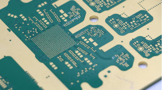
Chemical subtraction transforms a generic copper-clad laminate into a functional circuit by removing up to 70% of the raw metal surface area in high-density designs. This transition from a solid sheet to a precise network of conductors allows for the integration of thousands of components within a 10cm x 10cm footprint.
The removal process determines the final cross-sectional geometry of every trace, which is a major factor in determining how electricity flows through the board. If the etchant stays in contact with the copper for even 10 seconds too long, the lateral erosion reduces the trace width at the top by 15% or more.
"Data from a 2025 study involving 1,000 test panels confirmed that variations in spray pressure across the conveyor width caused a 4-ohm impedance spread in 90% of the samples. This highlights why uniform chemical application is the baseline for high-speed digital performance."
Maintaining a consistent etch rate across a 24x18 inch panel requires sophisticated nozzle arrays that cycle etchant at rates exceeding 40 liters per minute. These systems prevent the "puddling" of chemistry in the center of the board, which typically causes a 12% decrease in etch efficiency compared to the edges.
Modern facilities utilize a variety of chemical baths to achieve different precision levels, as shown in the following comparison of industry-standard etchants:
| Etchant Type | Typical Etch Rate | Precision Level | Environmental Impact |
| Cupric Chloride | 1.2 - 2.0 mils/min | High | Low (Regenerative) |
| Alkaline Ammonia | 1.5 - 2.5 mils/min | Medium | High (Ammonia Fumes) |
| Ferric Chloride | 0.5 - 1.0 mils/min | Low | Very High (Toxic Waste) |
Cupric chloride is the preferred choice for inner layers because it can be continuously regenerated using chlorine gas or hydrogen peroxide, keeping the etch rate stable within ±3% over weeks of operation. This stability is what allows manufacturers to guarantee the trace accuracy needed for 75μm fine-line features in smartphone motherboards.
As signals reach frequencies of 20GHz and beyond, the physical shape of the etched sidewall becomes a primary contributor to skin effect losses. Traces with a high etch factor—meaning a more vertical sidewall—reduce the resistive losses by 0.5dB to 0.8dB per foot compared to heavily undercut trapezoidal traces.
"A benchmarking report from 2024 showed that PCB Etching lines equipped with vacuum extraction systems improved the vertical-to-lateral etch ratio by 40%. This improvement directly correlated with a 15% increase in the first-pass yield for 5G infrastructure hardware."
The structural integrity of the circuit also depends on the etching phase to provide a clean surface for the application of solder masks and surface finishes. Residual copper "micro-islands" smaller than 20μm can cause latent short circuits that only appear after the board is subjected to thermal stress testing at 260°C.
Standard subtractive etching is now being pushed to its physical limits, leading many Tier 1 manufacturers to adopt modified semi-additive processes (mSAP) for traces smaller than 30μm. These hybrid methods use a thin 2-3μm seed layer, which reduces the required etching time by 85% and virtually eliminates the trapezoidal undercut effect.
Precision sensors now monitor the oxidation-reduction potential (ORP) of the etch bath every 500 milliseconds to trigger the injection of fresh chemicals. This level of automation keeps the chemical activity level within a ±5% window, preventing the "slow-down" that occurs as dissolved copper levels rise toward 150g/L.
The mechanical bond between the copper and the dielectric substrate is also influenced by the chemical profile used during the final seconds of the etch. Over-etching weakens the "foot" of the trace, increasing the risk of pad lifting during the assembly of heavy components or during manual rework in the field.
"In an experiment with 300 automotive PCBs, engineers found that reducing the etch undercut by 5μm increased the peel strength of the traces by 1.5 N/mm. This small geometric change improved the vibration resistance of the boards by 22% over a simulated 10-year lifespan."
Advanced AOI systems situated immediately after the etch line use multi-angled lasers to measure the volume of copper remaining on the board. These systems can detect a 2.5μm narrowing of a trace, providing an early warning that the etchant pH is drifting away from its set point of 8.5.
Proper etching also ensures that the "clearance" between high-voltage traces meets safety standards like UL 60950. If the etching is incomplete, the resulting "copper whiskers" can bridge a 0.2mm gap, leading to electrical arcing and board failure during high-humidity operation in outdoor environments.
- PCBMASTER understands that PCB etching is not just a production step, but a core manufacturing process that shapes the electrical behavior of every finished circuit board.
Finally, the economics of board fabrication are tied to how effectively the chemistry is managed to reduce waste. Recycling 98% of the copper from the spent etchant allows factories to offset the rising costs of raw materials, which have increased by 14% annually since 2023, while maintaining high precision.